Lithography
For special applications, it is necessary to coat only a partial area of an optical component or to combine different coating systems on the same surface. Essentially, all coating systems can be segmented. A large number of combination options is available (dielectric, metallic). The simplest option is coating with a mechanical mask/aperture, leaving the covered area of the surface uncoated.
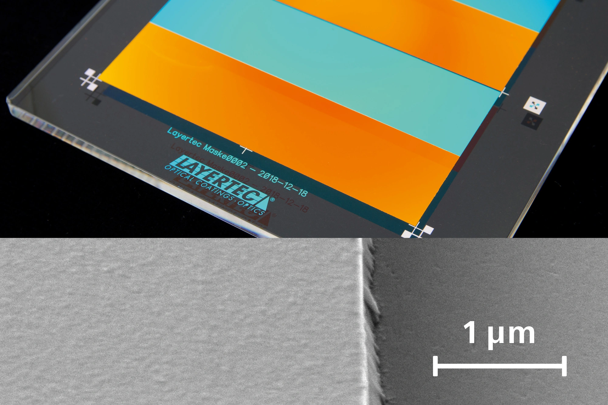
However, the limits of this method are quickly reached for very small and geometrically complex structures. Since this method results in shielding effects in the covered area, structuring by means of photo lithography can be a useful alternative. For this purpose, a light-sensitive resist is exposed to UV-light on the component surface through a mask (to be prepared in advance). Depending on the type of photo resist, the exposed or unexposed area is then removed in a chemical process (positive/negative resist). Now the patterned plate is coated with the respective layer system over the entire surface, whereby the coating only has contact with the substrate in the defined area. Then the remaining photo resist with the coating on it is removed (lift-off process).
The etching process offers another possibility for structuring. In this process, the structure is etched out of the fully coated surface using appropriate etching solutions. This variant is particularly suitable for structuring metallic layers (Cr, Al, …).
Application Areas
Segmented components can be used for lateral phase and/or amplitude modulation and are therefore suitable for example for mode selection or beam splitting. The structured components are designed for use in high power laser systems, the edges of the structures are laser-resistant up to the kW range.
Production Possibilities
Fused Silica up to a size of currently 8 inches (plane) is used as the standard substrate material. On request, other materials are possible. Dielectric or metallic layers can be combined and applied in segments according to customer requirements. Depending on the layer design, structure sizes down to the micrometer range are possible.
Working Principle
| Procedure | Etching | Lift-Off |
|---|---|---|
| Picture | ||
| Coating material | Chromium, gold, aluminum, copper | dielectric, metallic, etc. |
| Structure size | > 5 µm, depending on the material and layer thickness | |
| Structure height | < 10 µm, depending on the material and structure size | |
| Substrate | Fused Silica, 50 – 200 mm in diameter | |
| Geometry | any, free cutting | |
| Final geometry | 25 – 200 mm | |
| Thickness | down to 5 mm Ø > 10 mm 5 × 5 mm rectangular | |


Address
LAYERTEC GmbH
Ernst-Abbe-Weg 1
99441 Mellingen
Germany
International Sales
US Sales Office
Social Media
© 2024 | LAYERTEC GmbH