Measurement Tools for Testing Substrates
Surface Form Deviations
Any machined substrate exhibits surface form deviations from its theoretical design. The effect of these deviations on the functionality of the optics can be categorized with respect to the spatial dimension of the deviations. The following section refers to deviations of the optically active surface.
The inverse length of this spatial dimension – the spatial frequency – is used to mathematically describe the different kinds of deviations. A rough classification of deviations distinguishes between Form (low spatial frequencies), Waviness (mid-spatial frequencies) and Roughness (high spatial frequencies).
Form deviations affect the wavefront of the passing light while leaving the direction of propagation nearly unchanged. They lead to a distortion of the image or a significant alteration of the focal intensity distribution near the optical axis.
Waviness deviations also conserve the total energy of the propagating beam but mainly affect focal regions away from the optical axis. For example, periodical deviations in this frequency band can give rise to the formation of parasitic secondary foci.
Finally, roughness affects the propagating wavefront on spatially small regions. These disturbances lead to an effective scattering of energy off the direction of the main beam. Thus, there is a widespread intensity background resulting in a reduction of image contrast.
A quantitative distinction of form, waviness and roughness involves different optical and geometrical parameters, mainly the operating wavelength as well as numerical aperture and focal length. Thus, the same surface form deviation may lead to a significantly different optical behavior when used in different applications.
Surface Form Measurement
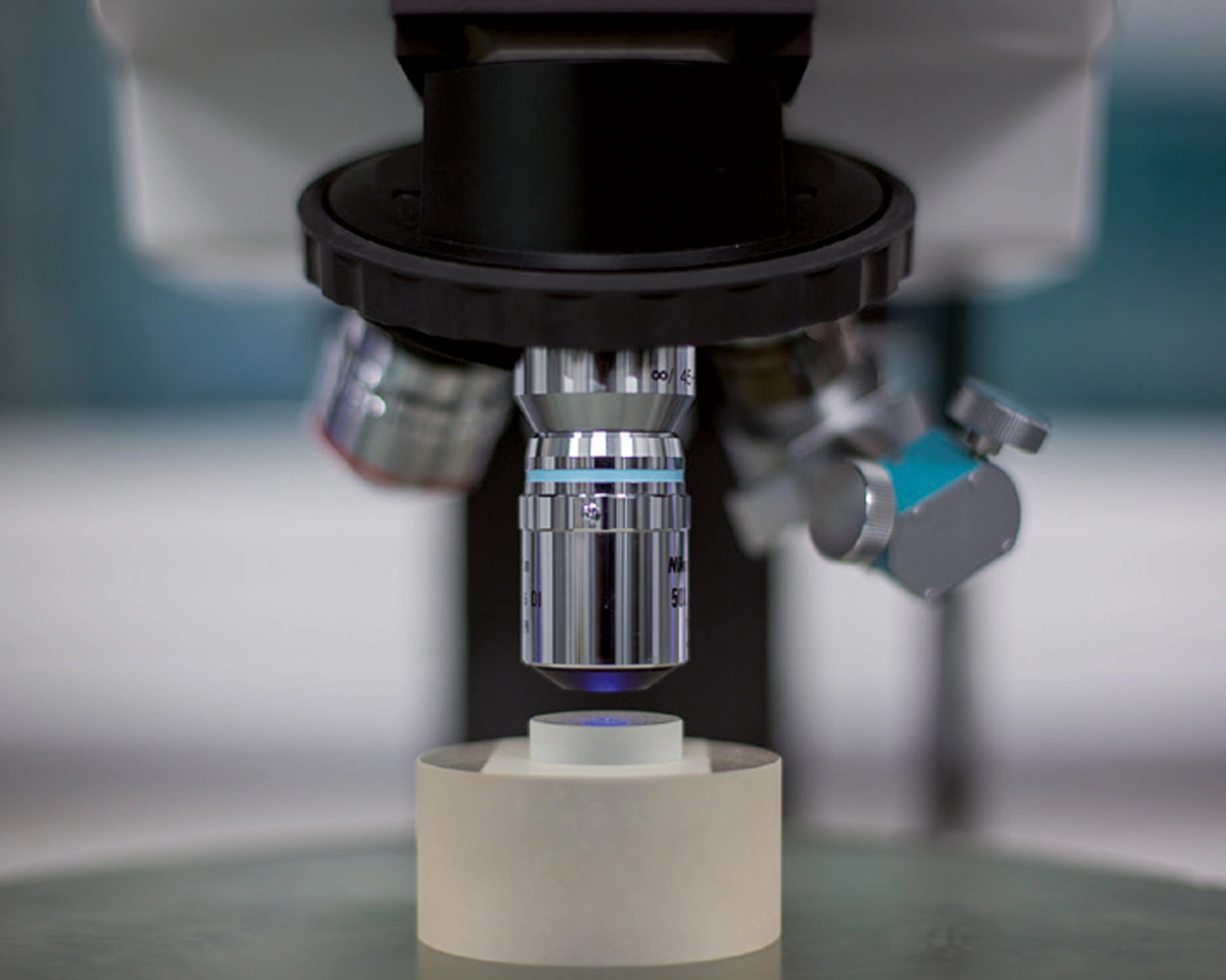
For the measurement of surface form deviation, LAYERTEC is equipped with laser interferometers and special interferometer set-ups for plane, spherical, cylindrical, aspherical and parabolic surfaces. Additionally, a tactile measurement device (Taylor Hobson PGI 1240 Asphere®) is available for general aspheric and ground surfaces. Besides the purpose of quality control, surface form measurement is a key function for the zonal polishing technology established at LAYERTEC.
Abbreviations
- P-V: The peak-to-valley height difference
- ROC: Radius of curvature of a spherically or cylindrically curved surface.
- λ: operating wavelength of the laser interferometer (e.g. 546 nm). The P-V value is stated in a fractional amount of λ. The actual value of λ is stated in measurement reports.
For detailed information about the standards concerning specification of surface form deviation please see ISO 10110-5.
Accuracy of Interferometric Measurements
Without special calibration procedures, the accuracy of an interferometric measurement is only as accurate as the reference surface. Calibration can increase the accuracy by a factor of 2 or more. Furthermore, the accuracy is influenced by the size of the measured area and in case of a curved surface by the radius of curvature itself. The accuracy values stated as “P-V better than …” in the following articles are guaranteed values. Very often accuracies of λ/20 or better will be achieved.
Standard Measurements
In general, the form tolerance of spherical and plane optics with diameters Ø ≤ 100 mm can be measured with an accuracy of P-V better than λ/10 by using ZYGO® Fizeau interferometers. To cover a measurement range of ROC = ±1200 mm over an aperture up to Ø = 100 mm, LAYERTEC uses high precision Fizeau objectives. In many cases, a higher accuracy up to P-V = λ/30 is possible. Measurement reports can be provided on request.
Large Radius Test (LRT)
Surfaces with radii of curvature above ±1200 mm are tested with a special Fizeau zoom lens set-up called Large Radius Test (LRT). This set-up was developed by DIOPTIC GmbH in cooperation with LAYERTEC. Its operating range is ROC = ±2000 … ±20 000 mm at working distances lower than 500 mm. The accuracy is guaranteed as P-V = λ/8 over Ø ≤ 100 mm, but typically it is better than P-V = λ/15. LRT has the advantages that only one Fizeau-objective is needed to cover a wide range of radii of curvature and that the working distance is kept small. This reduces the influence of disturbing air turbulences during the measurement.
Surface Roughness Measurement
In many applications, scattered light represents a crucial restriction to the proper operation of an optical device. On the one hand, scattered light reduces the intensity of the light propagating through the system, leading to optical losses. On the other hand, it also leads to a noise background of light reducing the overall contrast of imaging optics. The amount of scattered light produced by an optic is mainly determined by its surface roughness. Thus, requirements to the surface roughness are often necessary to guarantee the proper operation of a device. For a quantitative comparison, the RMS roughness is a widely-used measure to specify optical surfaces. It is defined as the root-mean-square of the surface height profile z:

Here the letter 'R' indicates line scans according to ISO 4287 while the letter 'S' refers to the evaluation of a scan on a two-dimensional measurement area as described in ISO 25178. The scan field size (maximum spatial frequency) as well as the resolution of the measurement set-up (minimum spatial frequency) affect the numerical value of Rq and Sq. For that reason, the specification of an RMS roughness value requires the specification of the underlying band of spatial frequencies as well. Often, technical drawings are lacking information on the frequency band and thus become meaningless. By using the power spectral density (PSD) of a surface, the distribution of the surface roughness with respect to the spatial frequencies becomes obvious. The RMS value of a surface simply follows from integration of the PSD over the given spatial frequency band. Generally, the scattered light of optical surfaces produced for the UV-NIR spectral range is dominated by spatial frequencies ranging from 0.01 to 10 µm-1.

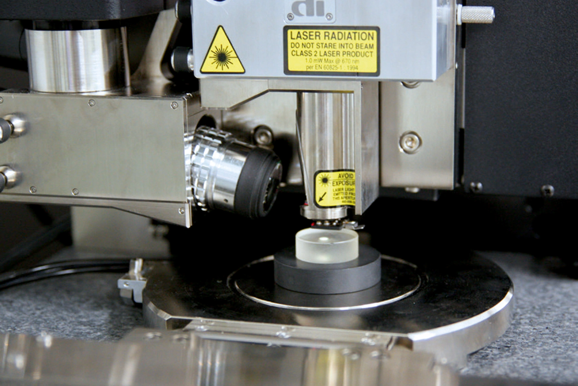
At LAYERTEC, different phase shifting and phase-shift masking optical surface profiler (Sensofar®, 4DTechnology®) and an atomic force microscope (AFM) DI Nanoscope 3100® are used to cover the given frequency band. The optical profilers cover low spatial frequencies and have an acquisition time of a few seconds. It is used for the general inspection of the polishing process and is able to identify surface defects and inhomogeneities. The AFM addresses high spatial frequencies using scan field sizes of 2.5 × 2.5 µm² and 25 × 25 µm² and has an aquisition time of 10 to 30 minutes. Therefore, it is used primarily for the development of polishing processes. It further serves to monitor the LAYERTEC premium-polishing process and especially optics for UV applications with Sq < 0.2 nm (spatial bandwidth: 7 – 1200 nm) with respect to quality control. Measurement reports are available on request.
Measurement Systems for Testing Substrates
Large Aperture Metrology
Especially for laser optics with large dimensions, LAYERTEC uses a high performance Fizeau interferometer and a Twyman-Green interferometer within the following measurement ranges:
- Plane surfaces: Ø ≤ 300 mm with an accuracy up to λ/20 (633 nm) and Ø ≤ 600 mm better than λ/10
- Spherical surfaces: Ø ≤ 600 mm with an accuracy better than λ/10 (633 nm)
- Parabolic surfaces: Ø ≤ 300 mm full aperture measurement with an accuracy up to λ/10 (633 nm)
Contactless Metrology
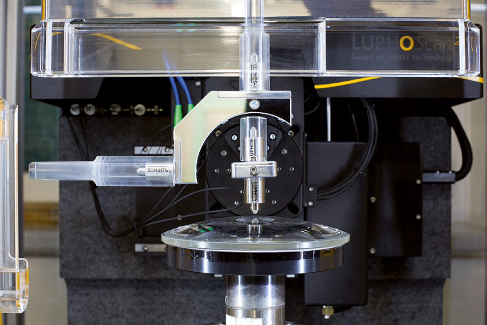
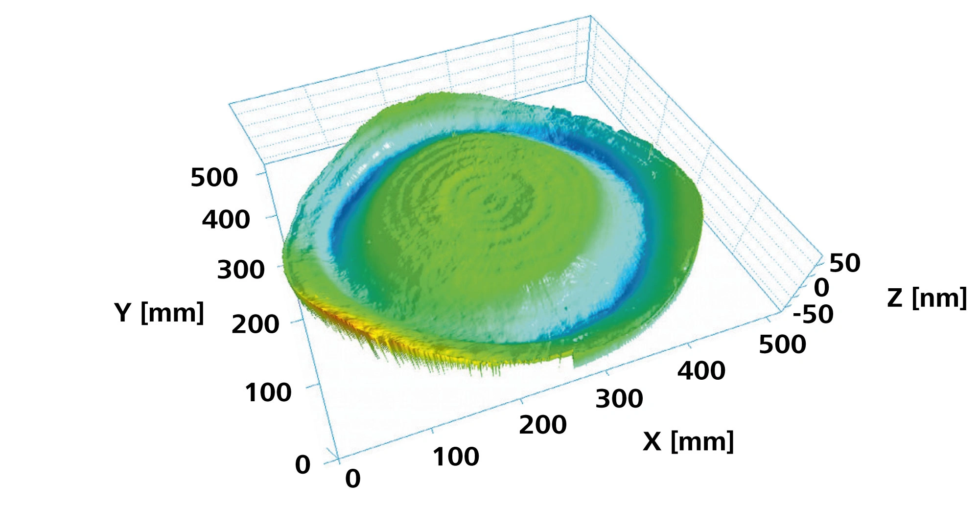
The metrology system LuphoScan®, developed by Luphos GmbH, allows an ultra-high precision measurement of distance and surface form. The unique system combines many advantages of other distance measurement systems without their disadvantages of necessary contact, small working distance or tiny working range. This technology allows the determination of the topology of different objects down to the nanometer range.
Highly reflective objects as mirrors or metal coated substrates can be measured as well as transparent objects providing only weak reflectance (glass lenses, substrates).
Due to its measurement range, it is possible to resolve structures of up to 1 mm height with a precision of ±5 nm. Especially, topological errors of aspheric surfaces can be exactly determined and used for a correction of the form parameters during the polishing process.
Tactile Surface Profiler
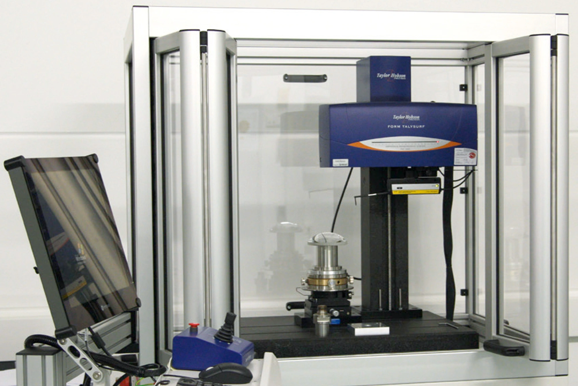
The Talysurf PGI 1240® is a tactile surface profile measuring tool used to characterize strongly curved surfaces. A small tip is in contact with the surface and moves along a line while its vertical displacement is measured.
The measurement principle is independent of surface topology or optical properties such as coatings or thin contaminations, which often prevent direct interferometry. The vertical accuracy depends on the gradient of the surface and can reach values of 500 nm, which corresponds to ≈ λ (633 nm).
LAYERTEC uses this tool for measurements of small to mid-size non-spherical surfaces up to a diameter of 200 mm.
Optical Profilometry

A 3D optical surface profiler (Sensofar®) based on a white light interferometer is used to visualize the surface form and roughness of our substrates. The profiler is furthermore applied for the characterization of surface defects and other structures in the range of sizes from 0.5 μm up to 100 μm.
Defect Analysis
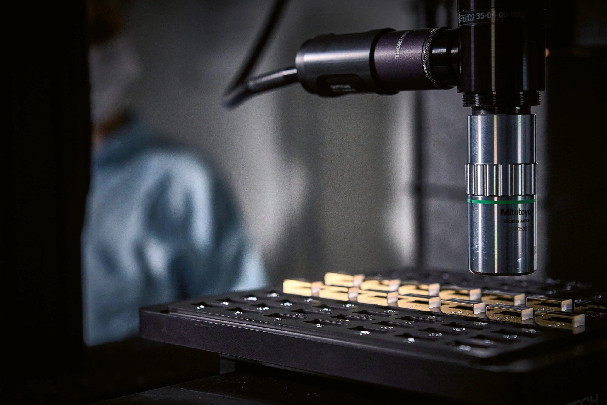
LAYERTEC has developed an automated measurement system for the detection and analysis of defects and scratches on optical surfaces. This system enables LAYERTEC to classify defect sizes according to ISO 10110-7. Thus, quality control procedures, such as final inspection, are facilitated, especially for high quality optics with defects specified below 25 µm.
Address
LAYERTEC GmbH
Ernst-Abbe-Weg 1
99441 Mellingen
Germany
International Sales
US Sales Office
Social Media
© 2024 | LAYERTEC GmbH