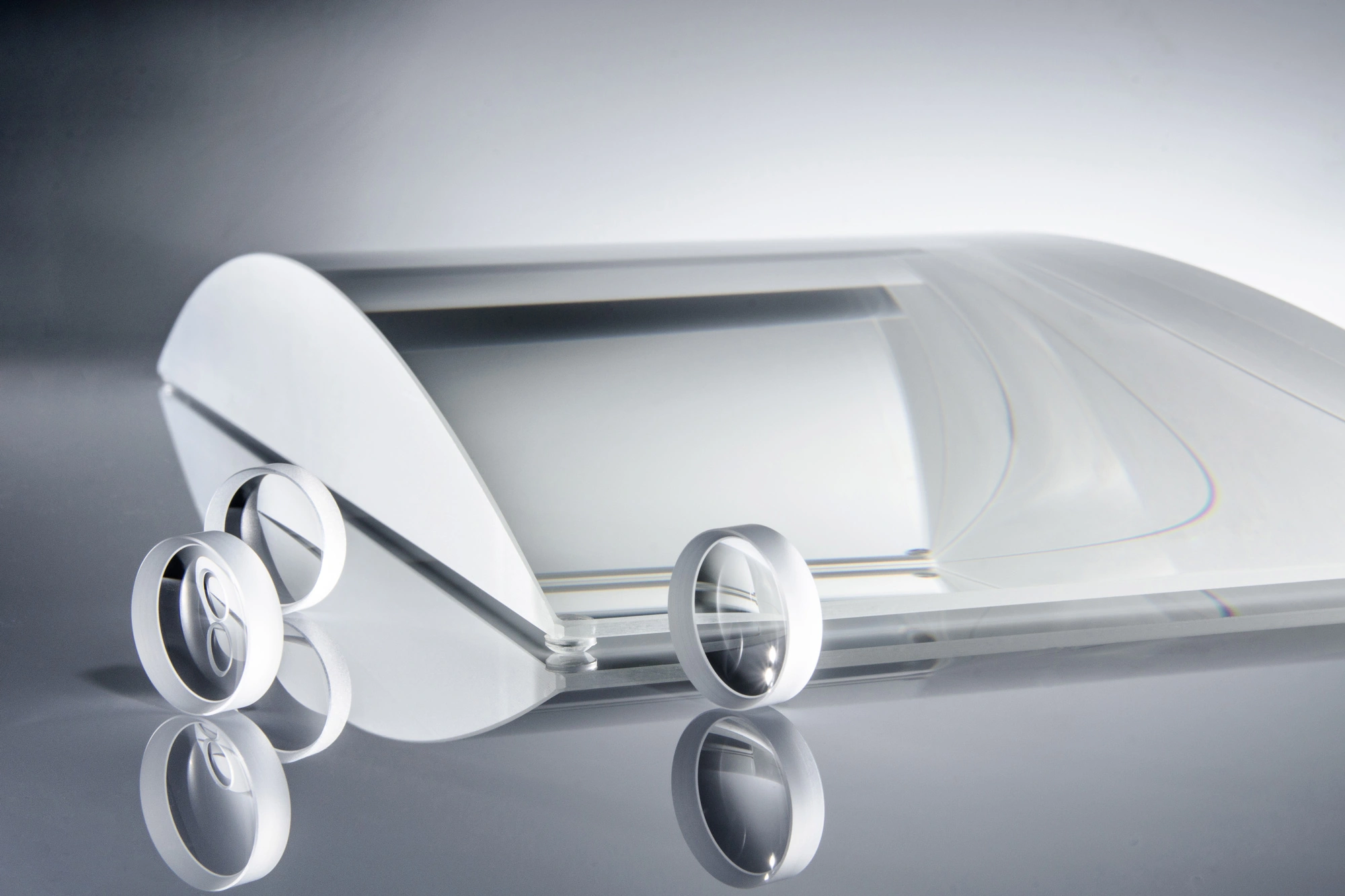
Optical Fabrication Methods
Manufacturing Technologies
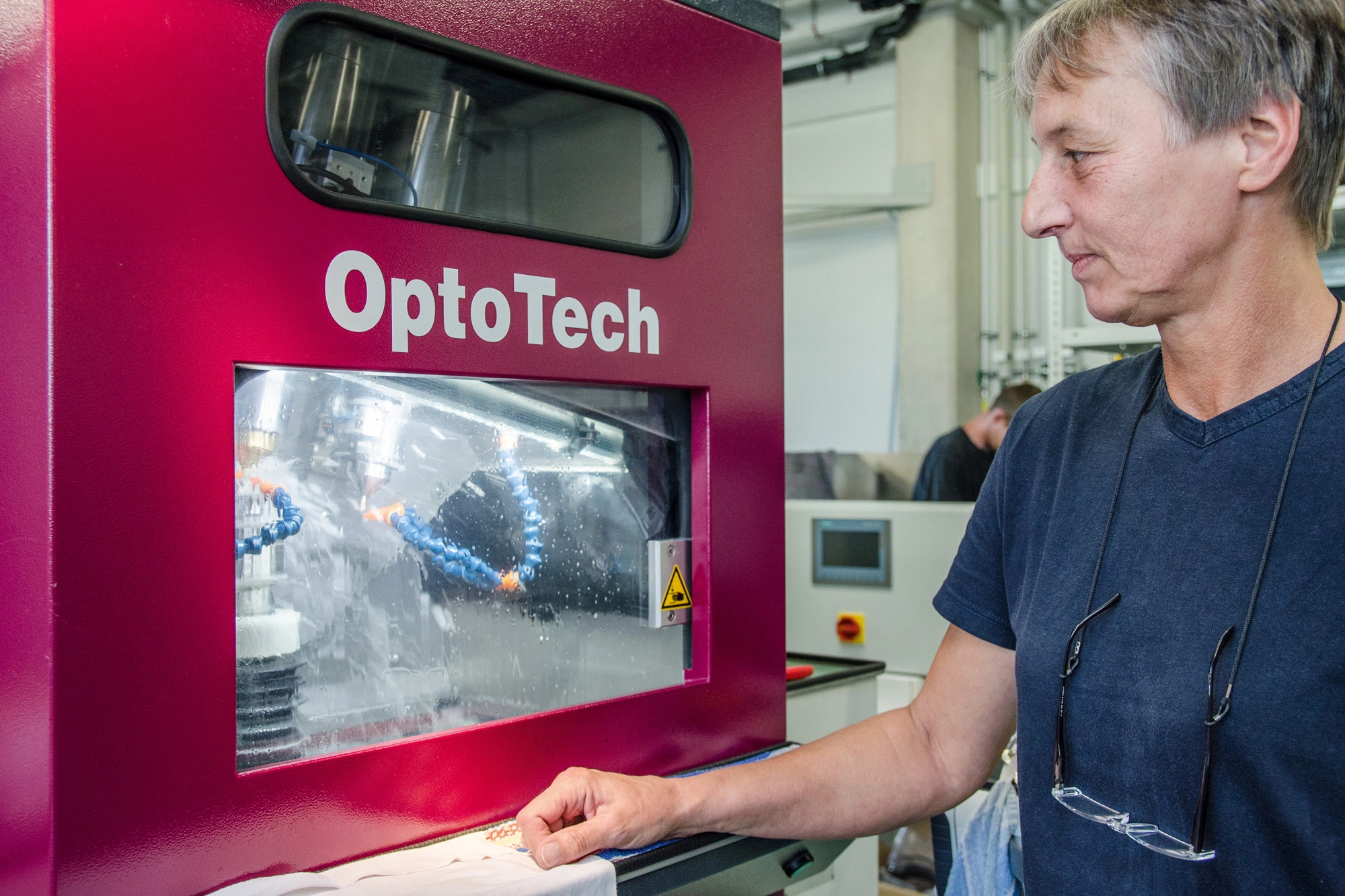
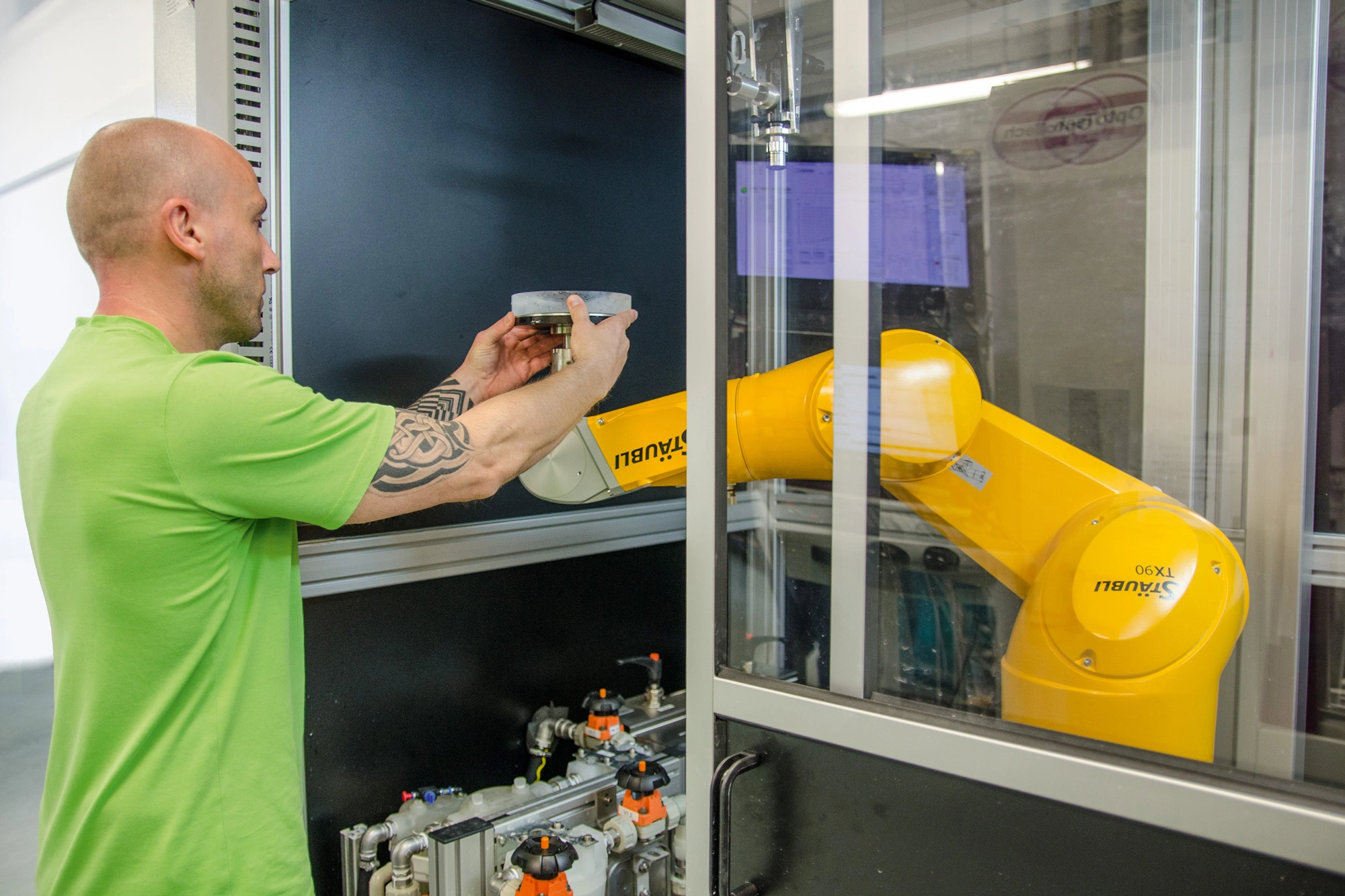
LAYERTEC has its own in-house precision optics facility where substrates with almost all geometries are manufactured. The optics are finished in our coating department according to individual customer requirements.
Traditional and Alternative Fabrication Methods
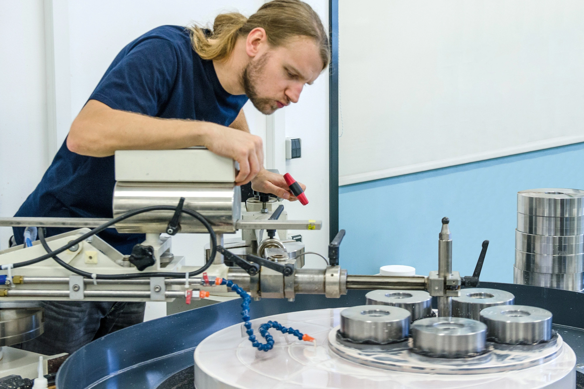

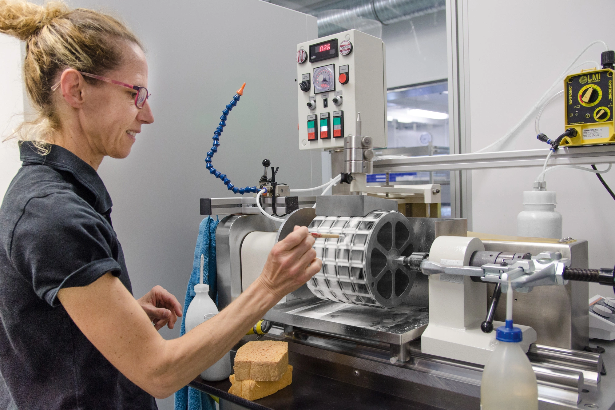
For the shaping of LAYERTEC optics, the production technologies grinding, lapping and polishing are mainly applied. Grinding is machining with geometrically undefined cutting edge. The cutting edges are irregularly arranged. The tool movement is rotary. The grain is bound in the tool. Lapping and polishing also belong to the machining processes with a geometrically undefined cutting edge. However, these are referred to as material removal by loose grains. The material is removed by a rolling movement of the lapping or polishing grains over the workpiece surface. From grinding to lapping to polishing, the grain sizes of the tools decrease. Each grain leaves surface imperfections in the order of the grain diameter during machining. The material removal of the next finer tool must be at least large enough to eliminate the surface defects of the previous one.
Besides the polishing of standard materials, LAYERTEC supports the polishing of various types of crystals such as YAG, KTP, LBO or BBO. This polishing technology also enables the careful handling and processing of small crystal sizes or extraordinary forms.
Ultrasonic Cleaning
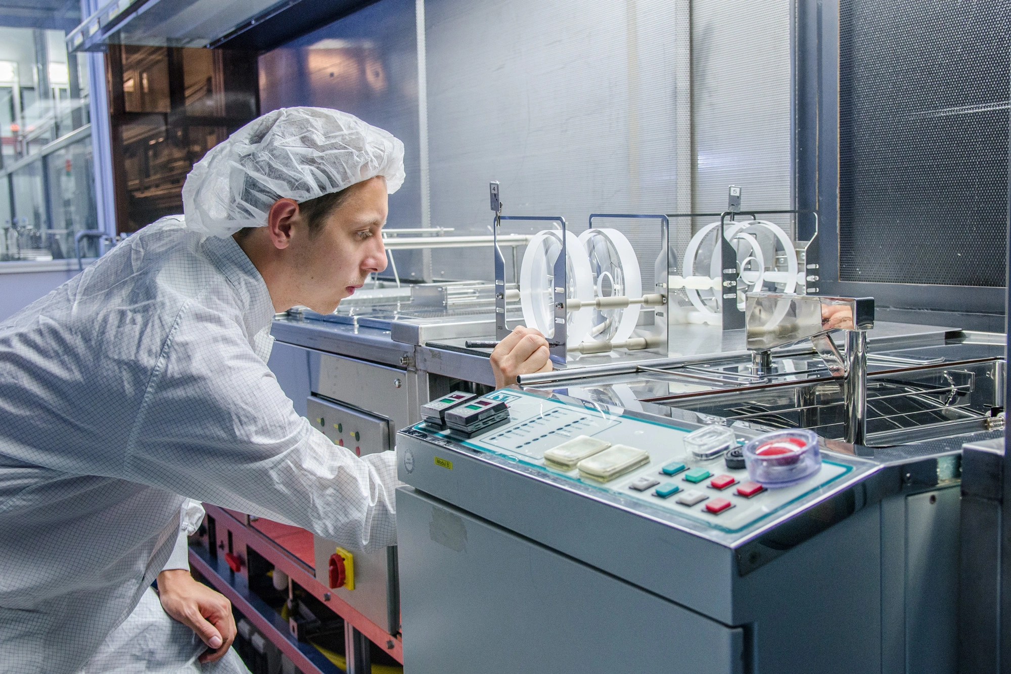
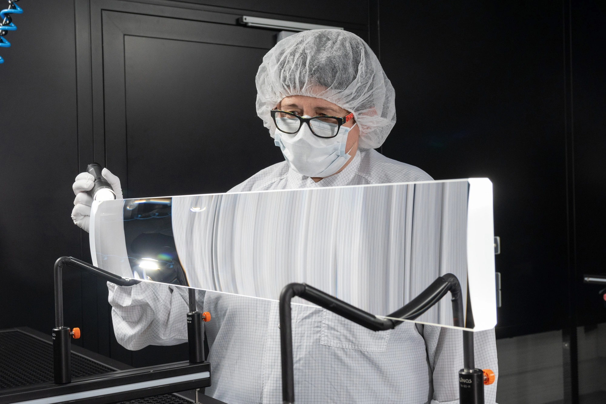
Ultrasonic cleaning represents the link between optics processing and coating in the production process. All substrates manufactured, purchased by LAYERTEC or provided by the customer must be absolutely clean before coating. Machining residues from optics production must be removed and the coating requirements for clean substrates must be met. LAYERTEC currently has 6 different ultrasonic cleaning systems for different requirements (e.g. crystal cleaning, pre-cleaning, fine cleaning, geometry dependent). The type of contamination determines the arrangement of the cleaning baths. Due to many years of experience in the field of ultrasonic cleaning, LAYERTEC has a broad knowledge base. Material properties of individual cleaners, temperatures as well as drying processes are always taken into account. Tailor-made solvents and the appropriate arrangement of cleaning baths can be used to deal specifically with a wide range of contaminants (emulsions, polishing agents, particles, fingerprints, salts, oils, greases, wax, water, paints, polymers, inks, etc.).
Plane Optics
Plane optics can be manufactured efficiently by using proven techniques of surface grinding, lapping and polishing.
Planar substrates are manufactured with diameters from 1.5 mm to 600 mm (round) or with edge lengths from 1 mm to 1200 mm (rectangular). Substrates down to a minimum thickness of 0.08 mm and any wedge can be produced. Special external geometries according to customer requirements are also possible.
Surface roughness of < 0.2 nm (usually measured for spatial structures in the range of 1 µm – 70 µm) is possible. Depending on the application wavelength, both defined and optimized surface roughnesses can be manufactured.
- Plane optics are made from the following materials:
- Fused Silica
- Crystalline Quartz
- YAG/LuAG
- CaF2
- ULE®
- Zerodur®
- Silicon
- BBO/LBO/KTP
- All commercially available optical glasses
- Toxic substrate materials, like ZnSe are not processed
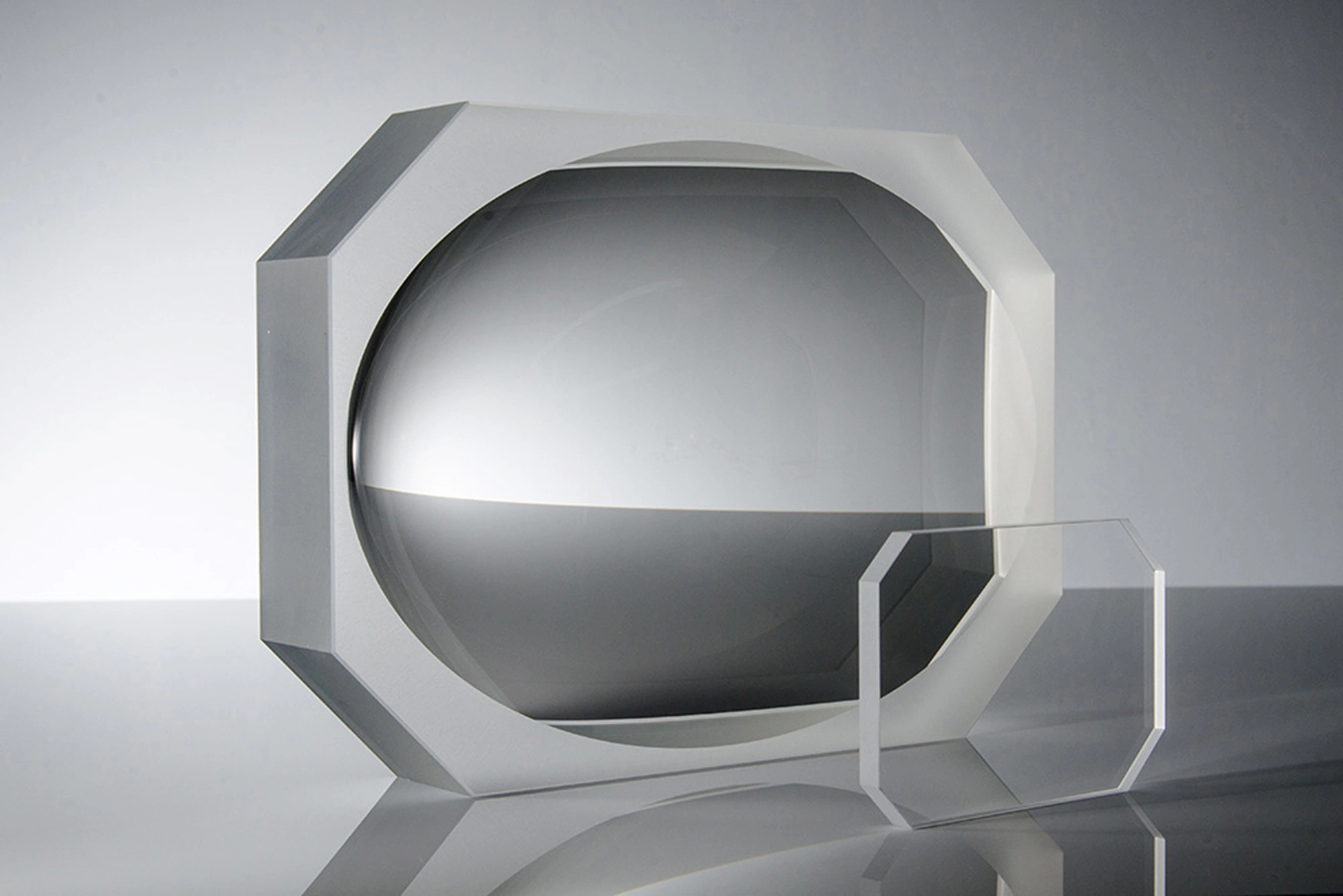
Spherical Optics
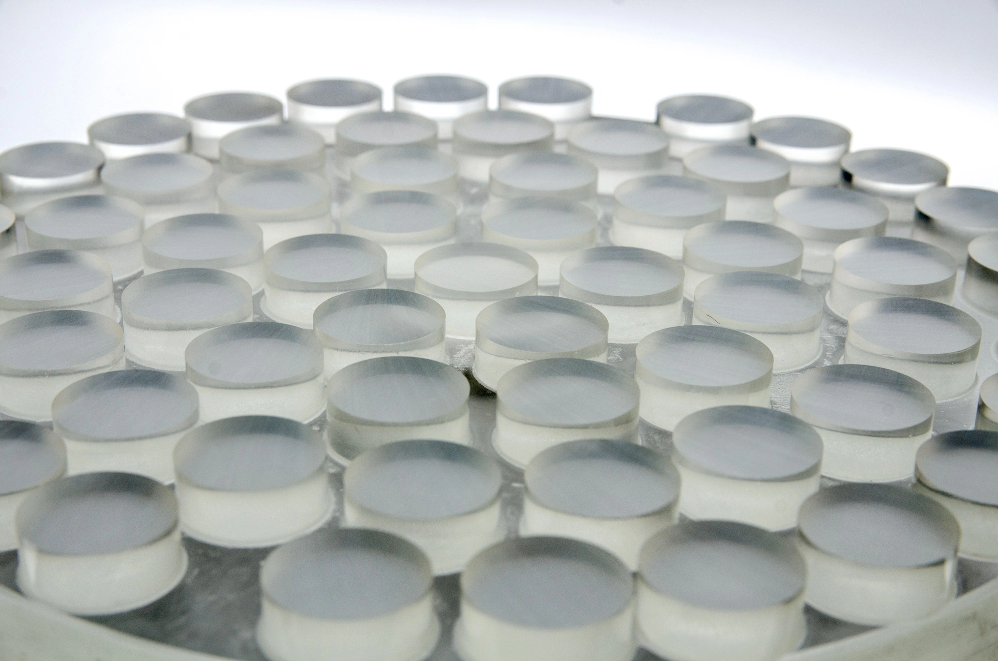
At LAYERTEC, single and double-sided curved substrates with convex or concave shapes are manufactured. The processing of a variety of optical glasses (e.g. Fused Silica, N-BK7®, ULE®) and crystals (e.g. Si, YAG, CaF2) is possible. Available radii of curvature vary from 5 mm to 100 000 mm. Manufacturing of substrate diameters from Ø = 3 mm to Ø = 600 mm (see also Large Optics on Large Scale Optics) is possible.
For Fused Silica, the following specifications can be achieved:
- Surface form deviations:
- Clear aperture up to 85 % of substrate diameter
- Further test areas on request
- 3/ -(0.2) (λ/10)
- 3/ -(0.1) (λ/20) on request
- Roughness Sq = 0.25 nm (for measurements with an optical profilometer taking into account spatial structures in the 1 µm – 70 µm range)
- Roughness Sq < 0.2 nm on request
Depending on the geometry, a centering accuracy of 1 arcmin and a radius tolerance of ±0.5 % can be achieved. We handle projects with special requirements on request.
Cylinder Optics
At LAYERTEC, cylindrical lenses can be manufactured in both concave and convex shapes, with a radius of curvature on one or both sides. Round or angular component shapes are possible. Cylindrical lenses can be made of all optical materials (e.g. Fused Silica, N-BK7®, SF6, CaF2).
Convex and concave radii in the range from r ≥ 7 mm to r = 1900 mm are produced as standard. Irregularities of up to λ/20 are possible.
Tactile and interferometric measurement technology guarantees production within the required tolerances.
| Fused Silica | CaF2 | |
|---|---|---|
| Clear aperture | 80 % | 80 % |
| Surface form tolerance (irregularity) | standard λ/4 on request λ/20 | standard λ/4 on request λ/10 |
| Surface imperfection tolerance | 25 mm × 25 mm standard 5/ 1 × 0.04 on request 5/ 1 × 0.025 | 12.7 mm × 12.7 mm standard 5/ 1 × 0.063 on request 5/ 1 × 0.04 |
| Specifications for other sizes on request | ||
LAYERTEC’s cylinder optics are used in aerospace, display manufacturing or laser generation, among others.
Aspheres & Free Forms
Plane and spherical optics can be efficiently manufactured by using traditional techniques of area grinding and polishing. The tool always works on a significant fraction of the substrate area at once. However, it is hardly possible to manufacture surface geometries that differ from regular forms like planes, spheres or cylinders. Using ultra precision CNC machinery, surfaces can be processed zonally, i.e. the tool works on one point at a time. The possible surface forms and tolerances are only limited by the precision of the machine and the measurement equipment. In contrast to the areal techniques, zonal processing usually works with a single piece per run only. Non-spherical optics can be divided into three categories: rotationally symmetric, off-axis and free form optics.
Rotationally Symmetric Non-Spherical Optics (Aspheres)
Although the term “asphere” may stand for any non-spherical optics, it is often restricted to rotationally symmetric optics. They are described by the following equation (cf. ISO 10110):
-rotationally-symmetric-non-sperical-optics-orig-1000-134-eed880fa.svg)
- Neglecting the aspheric coefficients leads to a profile of conic sections:
- Sphere: k = 0
- Ellipse: -1 < k < ∞
- Parabola: k = -1
- Hyperbola: k < -1

| Dimension | Tolerances | |
|---|---|---|
| Total Diameter | 25 – 560 mm | < 0.1 mm |
| Inspection Range | < 550 mm | |
| Total Thickness | < 100 mm | < 0.1 mm |
| Sagitta | < 50 mm | |
| Centering Error | < 50 mm | |
| Tilt Error | < 30'' | |
| Surface form tolerance (P-V) | λ/4 (λ/10 on request) | |
| Roughness* | < 0.3 nm | |
| * Valid for measurements with optical profilometer taking into account spatial structures in the 0.65 – 55 µm range | ||
Off-Axis Surfaces
An off-axis surface can be seen as a section of a bigger on-axis surface. The focal point still is on the original optical axis but not the center of the section. Instead, it is located off-axis. Off-axis surfaces derived from aspheres are described by the mentioned equation, the off-axis distance a and/or the off-axis angle α.

The focal length of the parent parabola (fparent) is measured from the vertex on the optical axis. For the off-axis parabola (OAP), an effective focal length (feff) is introduced. The off-axis distance is measured from the optical axis to the middle of the OAP. The radius R denotes the radius of curvature in the vertex of the parent parabola. The conic constant k is -1.
In principle, an off-axis substrate can always be mechanically cut from an on-axis substrate. The alternative way is direct manufacturing (parallel configuration). Depending on the size and tolerances, both ways are possible.
Basically, LAYERTEC’s off-axis surfaces are manufactured in the direct way. Manufacturing from the parent parabola is currently limited to Ø = 300 mm and is only carried out on request.
Please provide the following specifications when making inquiries:
- Geometry data
- Clear aperture
- Focal length (effective or parent parabola focal length)
- Off-axis angle or off-axis distance
- Material
- Necessary surface imperfection tolerance according to ISO 10110 (3/; 4/; 5/; etc.)
- Coating
Free Form Surfaces
In general, free form surfaces do not exhibit any symmetries. They are always customer specific and can be defined by an equation. Additional specification of tabulated sagitta values is highly recommend. Free form surfaces are manufactured as single pieces. With respect to machining, the production of an off-axis asphere from a single piece represents a free form as well. Table 3 shows LAYERTEC’s production dimensions and tolerances for free form surfaces.

| Dimension | Thickness | |
|---|---|---|
| Ø | < 300 mm | ±0.2 mm |
| w | < 300 mm | ±0.1 mm |
| l | < 450 mm | ±0.1 mm |
| α | < 45° | |
| te | < 80 mm | ±0.1 mm |
| d | ±0.1 mm | |
| Surface form tolerances (P-V) | λ/4 (λ/10 on request) | |
| Roughness | < 0.3 nm |
Materials
The surface imperfection tolerance and the final tolerances strongly depend on the material of the substrate. LAYERTEC uses a process optimized for Fused Silica. Materials like Zerodur®, ULE® or N-BK7® may be used in special cases.
Measurement
Measuring aspheric surfaces requires sophisticated devices. LAYERTEC applies 2 different measurement principles. See also page Surface Form Deviations.
- Single point interferometer:
Contactless measurement of the surface, measuring the surface point by point. Precision λ/4 on ≤ Ø 420 mm. - Interferometer with reference surface:
The surface is compared to a known reference surface. Precision < 50 nm, on Ø ≤ 300 mm. Concave surfaces preferred.
Special Surfaces
Particular applications in optics exhibit a demand for optical surfaces that are far away from flat, spherical or even aspheric surfaces. Thus, in the following such surfaces are referred to as special surfaces.
The fabrication of these special surfaces can typically not be addressed with conventional manufacturing technologies in optics. At LAYERTEC a local correction technique with a footprint of ≈ 1 mm in diameter is used. This allows the fabrication of profiles with typical lateral features above 1 mm. In the set-up the handled substrates are up to 400 mm in diameter. Surface profiles are applied with a typical fabrication error below 25 nm (along the z-axis). Furthermore, this technique allows a complete processing of the optical surface. In contrast to most local correction techniques there is no need for a safety margin around substrate edges.
Optical vortices are a well-known example of a special surface. They are mainly used in the generation of laser beams with a spiral phase. The structure of an optical vortex is exemplary shown in Fig. 16a. With respect to the manufacturing of a vortex the main feature of such a profile can be found in the edge, showing a typical height of several 100 nm. In the fabrication process the footprint of the local polishing tool smears out this edge. Fig. 16b shows the surface form deviation of a real substrate (30 mm in diameter) processed by LAYERTEC.


Another application of special surfaces can be found in the compensation of thermal lenses. In this case the respective wavefront error caused by a thermal lens is translated into a surface form deviation of a transmissive or reflective optical element. Such a surface is then applied to a real optics counteracting the thermal lens in the stationary working regime of the application. A typical example of the surface form of such an element is shown in Fig. 17.

Large Scale Optics
LAYERTEC offers large scale optics which are used for a variety of applications in industry (material processing, measurement, semiconductor industry, display production), science, medical and other areas. Processing technologies are offered for all common Fused Silica optics (special materials on request). LAYERTEC develops large optical components in cooperation with the customer from prototype to serial production. LAYERTEC has suitable measurement equipment to ensure the promised specifications.
- Optical Components
- Planar optics
- Spheres
- Cylinders
- Aspheres, off-axis parabola
- Free-form optics
- Accuracy and quality of surfaces
- Planarity up to λ/20
- Polishing level 4
- Roughness Rq ≤ 0.5 nm
- Surface defects down to 1 ppm of checking area
- Technologies for substrate fabrication
- CNC grinding up to 2000 mm
- Polishing (CNC and classical) up to 2000 mm
- Interferometry (flat and cylindrical surfaces) up to 2000 mm
- Roughness measurement (tactile and optical) up to 2000 mm
- Multi-sensor coordinate measuring up to 2000 mm
- Ultrasonic cleaning technology up to 1200 mm
- Optical Coating Technologies
- IAD up to 1200 mm
- Magnetron-sputtering up to 600 mm
- Characterization of optical coatings (OPO-CRD, PCI, LIDT)
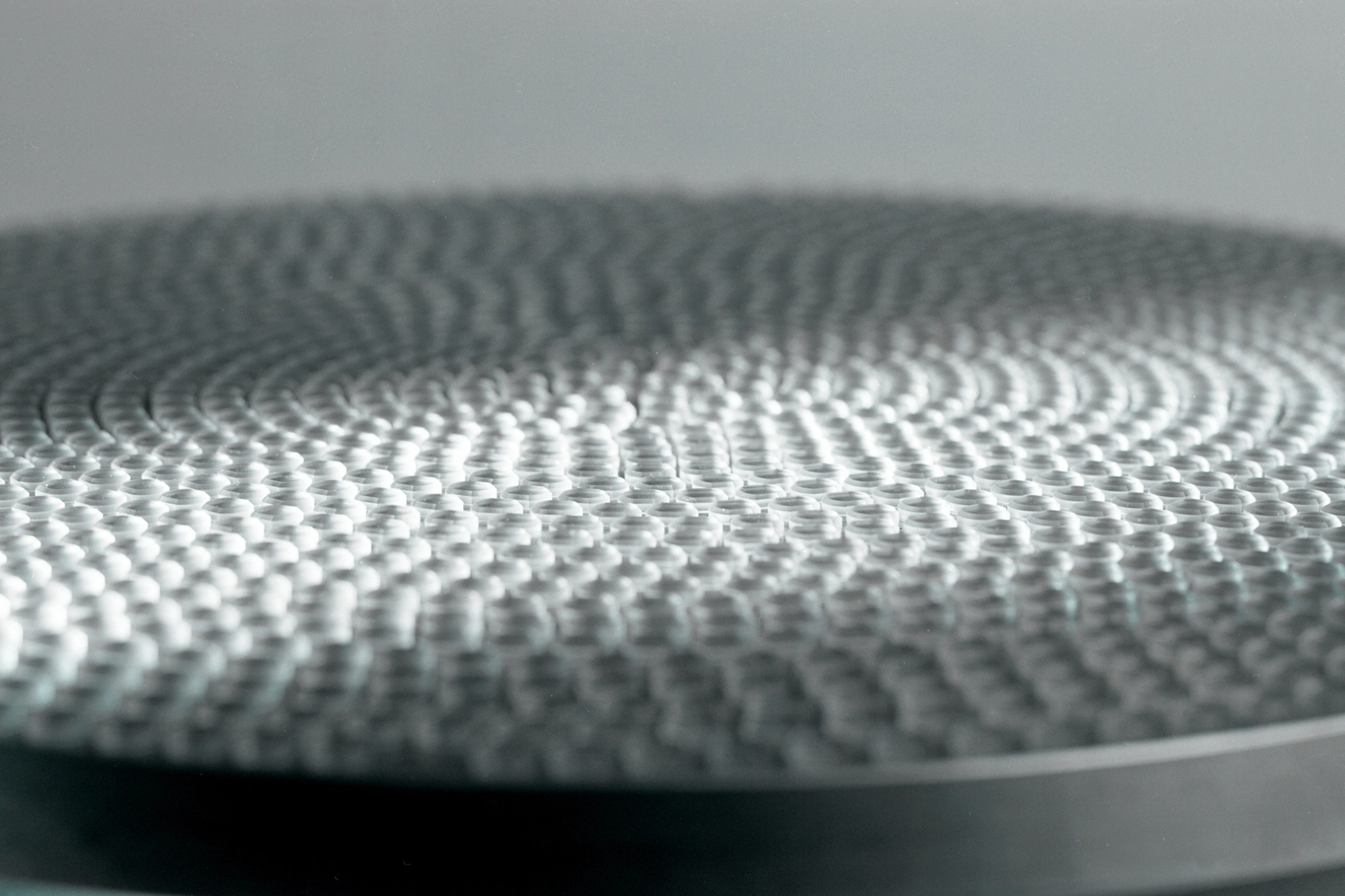
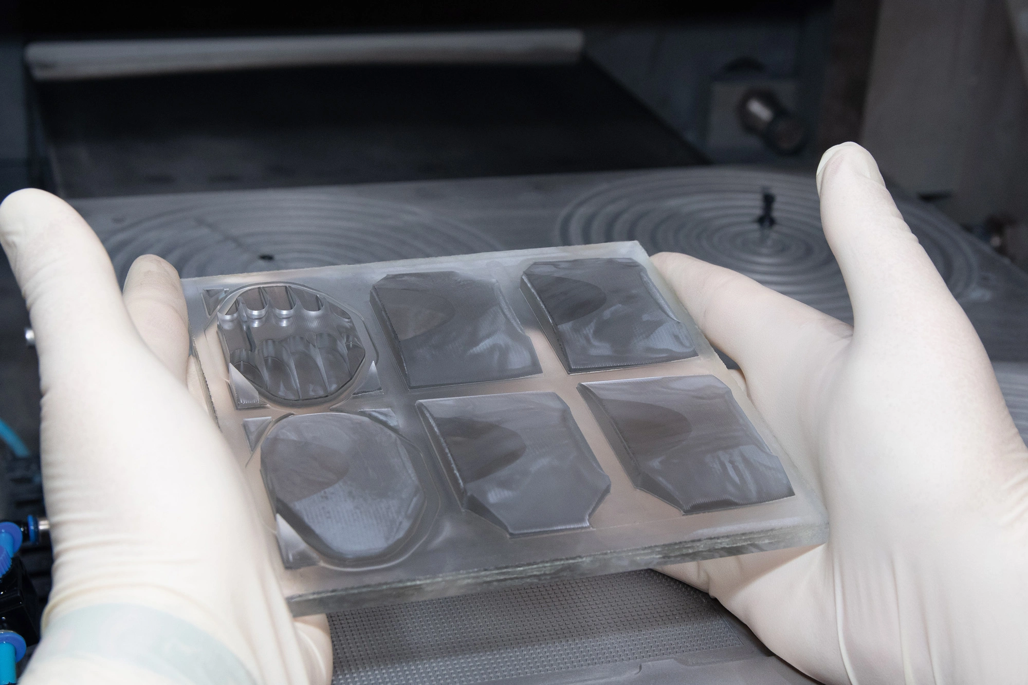
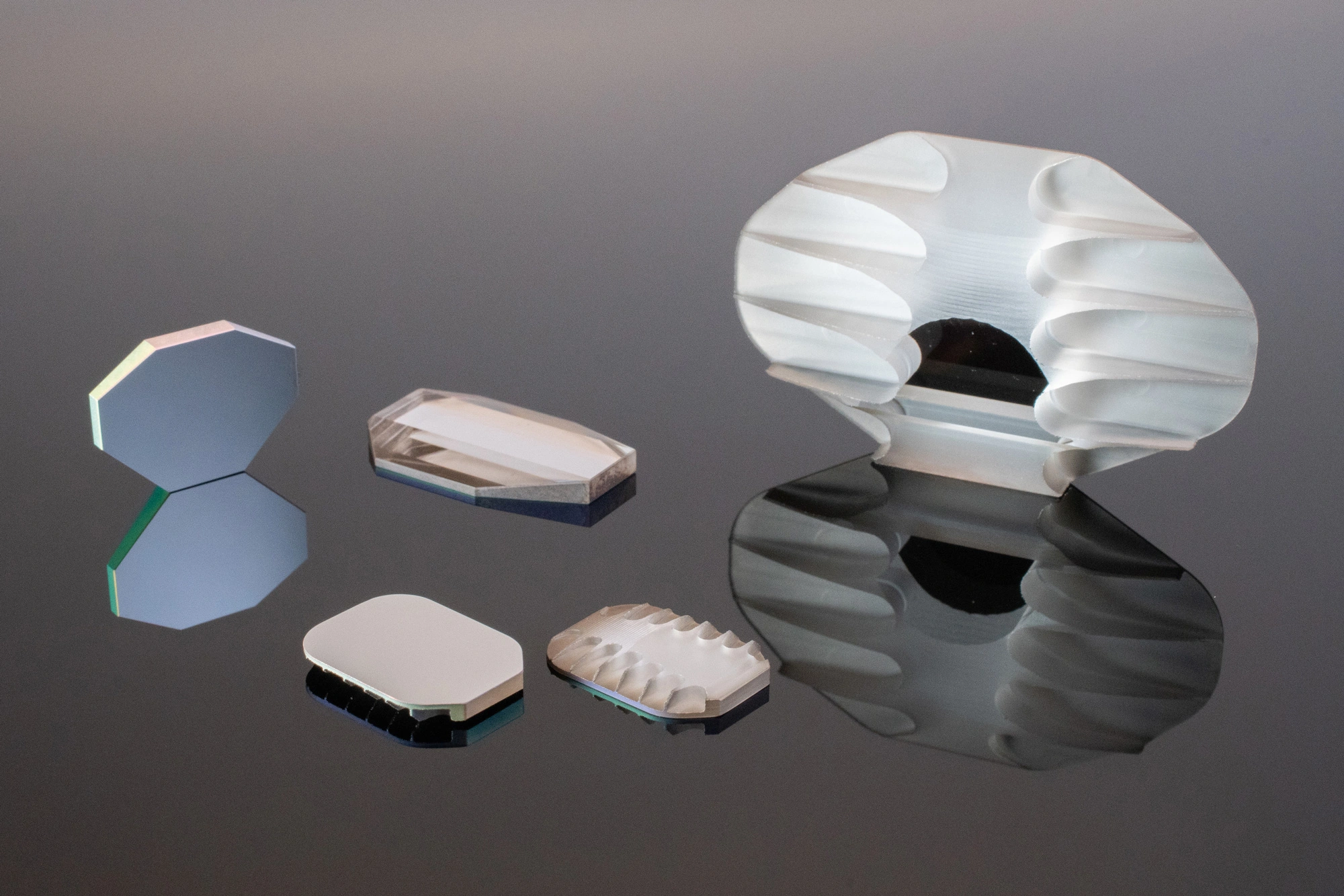
Scanning Mirrors & Lightweight Structures

Scanning mirrors are special deflection mirrors with an optical function surface. By rotating the mirror, the direction of the reflected beam can be changed. With a single mirror, a line can be scanned. With a combination of 2 scanning mirrors, whose axes of rotation are offset by 90 degrees, a two-dimensional surface can be scanned.
Various CNC machining technologies are available for the production of scanner mirrors. Standard scanner mirrors are not yet lightweight components, but normal "solid" mirrors with "normal" dynamic requirements. However, these can be optimized according to customer requirements in terms of weight (lightweight scanner mirrors) or speed of movement (high-speed scanner mirrors).
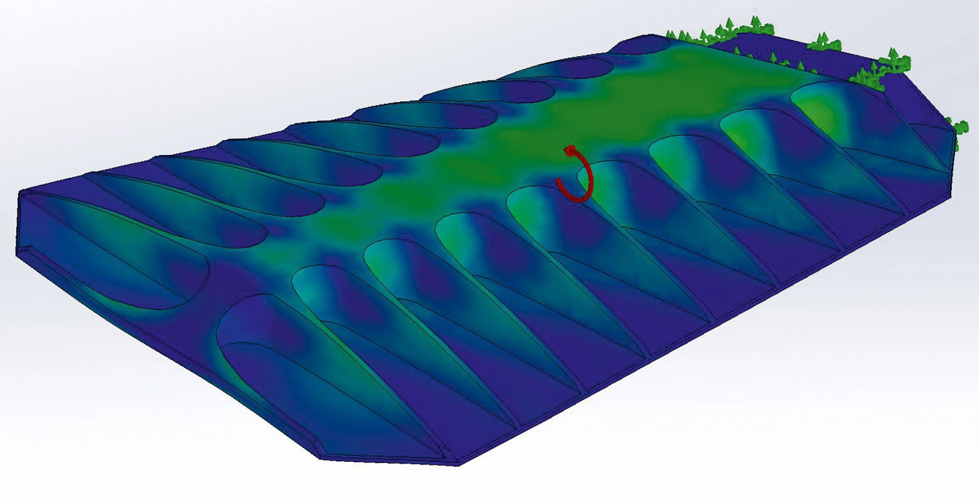
Lightweight and high-speed scanner mirrors are characterized by herringbone-like structures, which are responsible for reducing the mass moment of inertia by up to a factor of 4 (compared to "solid" material). The resonant frequency is increased by up to a factor of 1.5 by this step, and the dynamic deformation is reduced by up to a factor of 1.5. These special shapes are used when a very fast change in the direction of movement of the laser beam over the workpiece surface is desired.

| Fused Silica | Standard | Lightweight | High Speed | |||
|---|---|---|---|---|---|---|
| Limits for mirror sizes | small | large | small | large | small | large |
| Total width [mm] | 20 | 80 | 40 | 80 | 15 | 40 |
| Total length [mm] | 20 | 80 | 40 | 80 | 15 | 40 |
| Total thickness [mm] | 3.2 | 6.35 | 6.35 | 9.5 | 2.5 | 6.35 |
| Moment of inertia [g×mm²] | 100 | 8000 | 120 | 2000 | 13 | 120 |
| Resonance frequency in direction of rotation [Hz] | 15000 | 3000 | 8000 | 4000 | 20000 | 8000 |
| Max. Stress at 10 000 rad/s² [N/mm²]* | 0.03 | 0.8 | 0.005 | 0.1 | 0.03 | 0.06 |
| Form deviation at 10 000 rad/s² [nm] | 100 | 450 | 50 | 300 | 5 | 50 |
| * The angular acceleration of 10 000 rad/s² corresponds approximately to a frequency of 22 Hz when the amplitude is ±30°. This angular acceleration is an example value to indicate stress and deformation. The stress and deformation in the substrate are assumed to be linear with respect to angular acceleration. Thus, doubling the angular acceleration will lead to a doubled amount of dynamic deformation. Furthermore, the angular acceleration scales linearly with a change in the modulation amplitude and quadratically with respect to a change in frequency. | ||||||
Coating is done by magnetron sputtering, IBS or evaporation and can be customized according to customer requirements.
Etalons & Waveplates
Etalons
As a kind of Fabry-Pérot interferometer, the etalon is typically made of a transparent plate with two reflective surfaces. Its transmittance spectrum, as a function of wavelength, exhibits peaks of high transmittance corresponding to resonances of the etalon. Etalons are widely used in telecommunication, lasers and spectroscopy for controlling and measuring the wavelength of laser sources. LAYERTEC offers etalons of customized diameters and various materials depending on the wavelength range. Thicknesses down to 50 µm and a parallelism < 1 arcsec are possible subject to the diameter. Do not hesitate to contact us for the customized diameter and thickness you need.
| Thickness | Parallelism | |||
|---|---|---|---|---|
| Ø = 50 mm | Ø = 25 mm | Ø = 12.7 mm | ||
| Fused Silica | ≥ 200 µm | ≥ 100 µm | ≥ 50 µm | < 1 arcsec |
| YAG | ≥ 200 µm | ≥ 90 µm | ≥ 50 µm | < 1 arcsec |
| CaF2 | — | ≥ 300 µm | ≥ 100 µm | < 5 arcsec |
Waveplates
LAYERTEC offers customer specific retardation plates made of crystalline quartz. Due to requirements for mechanical stability, there is a minimum feasible thickness depending on diameter. Thus, there is a constraint with respect to the shortest available wavelength for a given waveplate order. For selected geometries LAYERTEC provides effective zero-order waveplates. These waveplates are made by combining two individual waveplates with alignment of the fast axis of one plate to the slow axis of the other. The resulting net retardation of this assembly is the difference between the two retardations. For two frequently requested diameters, examples are given below. Other diameters are available on request. Please contact us for further information.
| Order | Ø = 25 mm | Ø = 18 mm | Thickness Tolerance | Parallelism |
|---|---|---|---|---|
| λ/2 | Available wavelengths | |||
| K = 0 | — | λ > 1530 nm | ±1 µm | < 1 arcsec |
| K = 1 | λ > 720 nm | λ > 560 nm | ±1 µm | < 1 arcsec |
| K = 2 | λ > 450 nm | λ > 350 nm | ±1 µm | < 1 arcsec |
| λ/4 | Available wavelengths | |||
| K = 1 | λ > 860 nm | λ > 660 nm | ±1 µm | < 1 arcsec |
| K = 2 | λ > 500 nm | λ > 380 nm | ±1 µm | < 1 arcsec |
Address
LAYERTEC GmbH
Ernst-Abbe-Weg 1
99441 Mellingen
Germany
International Sales
US Sales Office
Social Media
© 2024 | LAYERTEC GmbH