Special Metallic Coatings (400 – 10 000 nm)
Chromium Coatings for Optical Applications
Chromium coatings are used for lithographic processes and other special optical applications. LAYERTEC offers chromium coatings with extremely low pinhole density on mask blanks and silicon wafers. Typical substrates sizes are 6 inch × 6 inch, but uncommon sizes up to diameter 600 mm are also possible. LAYERTEC uses specialized sputtering processes for very efficient industrial production. These processes are optimized for:
- Low pinhole density
- High optical density
- Low mechanical stress
- High electrical conductivity
Besides high volume coating manufacturing, LAYERTEC still maintains its capabilities for flexible production of small volumes such as OEM components or components for research and development. Do not hesitate to contact LAYERTEC regarding your special request.

Solderable Coatings
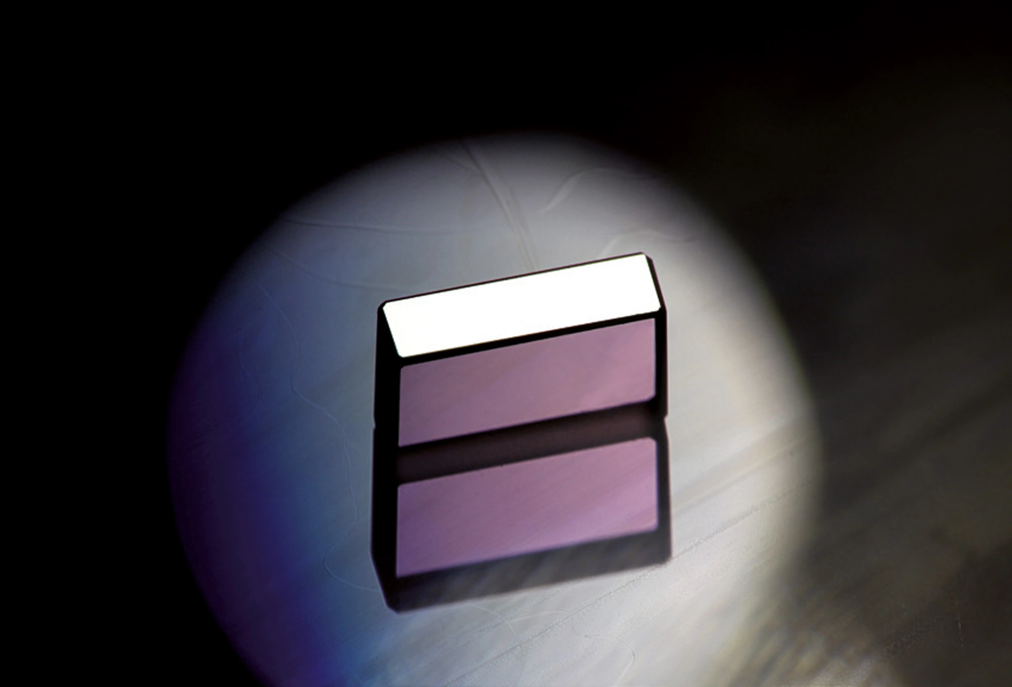
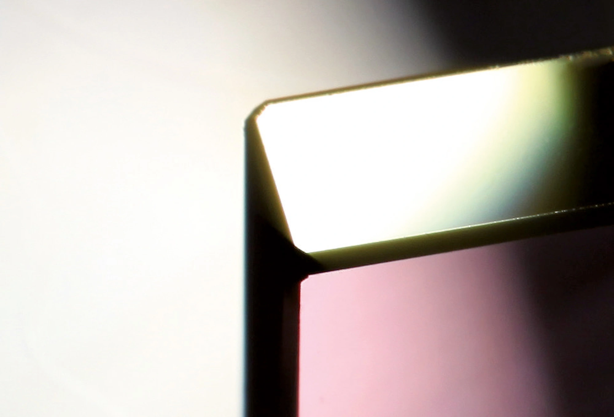
Soldering is one of the most important mounting techniques for optics which require excellent thermal contact to a heat sink. LAYERTEC has developed several coating designs containing gold and other metals which can be used for soldering of the optics. A very special problem is to solder coatings on components for high power applications. As an example Fig. 2 show a pump mirror which is coated with a solder layer system on the top side and with dielectric coatings on the front and rear surfaces. Extreme care must be taken to avoid metallic contaminations on the optical surfaces. Nevertheless, the solder coating has to cover the whole top surface of the substrate.

Partially Transmissive Gold Layers for Optical and Non-optical Applications

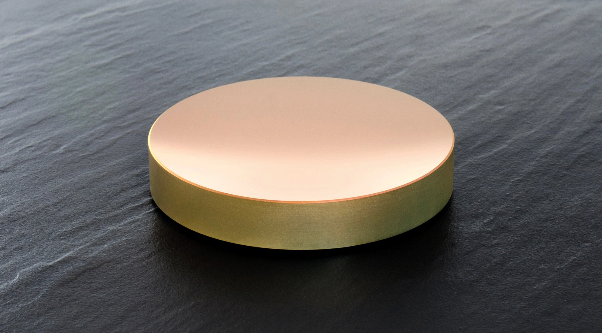
Gold coatings with a thickness of 10 nm to 50 nm can be used as partial reflectors or attenuators in the NIR spectral range. Fig. 5 shows transmittance spectra of gold layers with different thickness. Moreover, thin gold layers are also useful for non-optical applications. An example of such an application is the generation of single electron pulses. Thin metallic layers are irradiated with femto-second laser pulses. This results in the release of electrons. These electron pulses are generated with the repetition rate of the ultrafast laser. The pulse length of these electron pulses can be compressed to the attosecond range using a microwave cavity [1, 2]. Magnetron sputtering allows the manufacture of partially transmissive gold layers in the mentioned thickness range. The optical parameters of these coatings are very stable because gold is chemically inert. Please note that gold layers are soft and can be easily damaged mechanically.
Literature
[1] A. Gliserin, A. Apolonski, F. Krausz, P. Baum: “Compression of single electron pulses with a microwave cavity”; New Journal of Physics 14(2012) 073055 (18 pp)
[2] M. Aidelsburger, F. O. Kirchner, F. Krausz and P. Baum: “Single-electron pulses for ultrafast diffraction”; PNAS Vol.107, No.46, pages 19714-19719
Address
LAYERTEC GmbH
Ernst-Abbe-Weg 1
99441 Mellingen
Germany
International Sales
US Sales Office
Social Media
© 2024 | LAYERTEC GmbH